Thin-Film Microstrip and IPD Filters: Bare-Die RF Filters on Glass, Quartz and Alumina
At microwave frequencies an RF filter is less a component catalog choice than a transmission-line geometry problem. Once a filter topology — coupled line, hairpin, interdigital, combline, elliptic — is selected, the remaining variables are substrate dielectric, conductor quality, dimensional tolerance and packaging. Thin-film microstrip and integrated-passive-device (IPD) filters built on glass, fused quartz or alumina answer those variables differently from ceramic packaged filters and from waveguide assemblies, and they increasingly appear in switched filter banks, test instrumentation, point-to-point radio and mmWave front-ends.
This article explains how a thin-film filter is made, where its performance advantages come from, and how to specify one against packaged and LTCC alternatives.
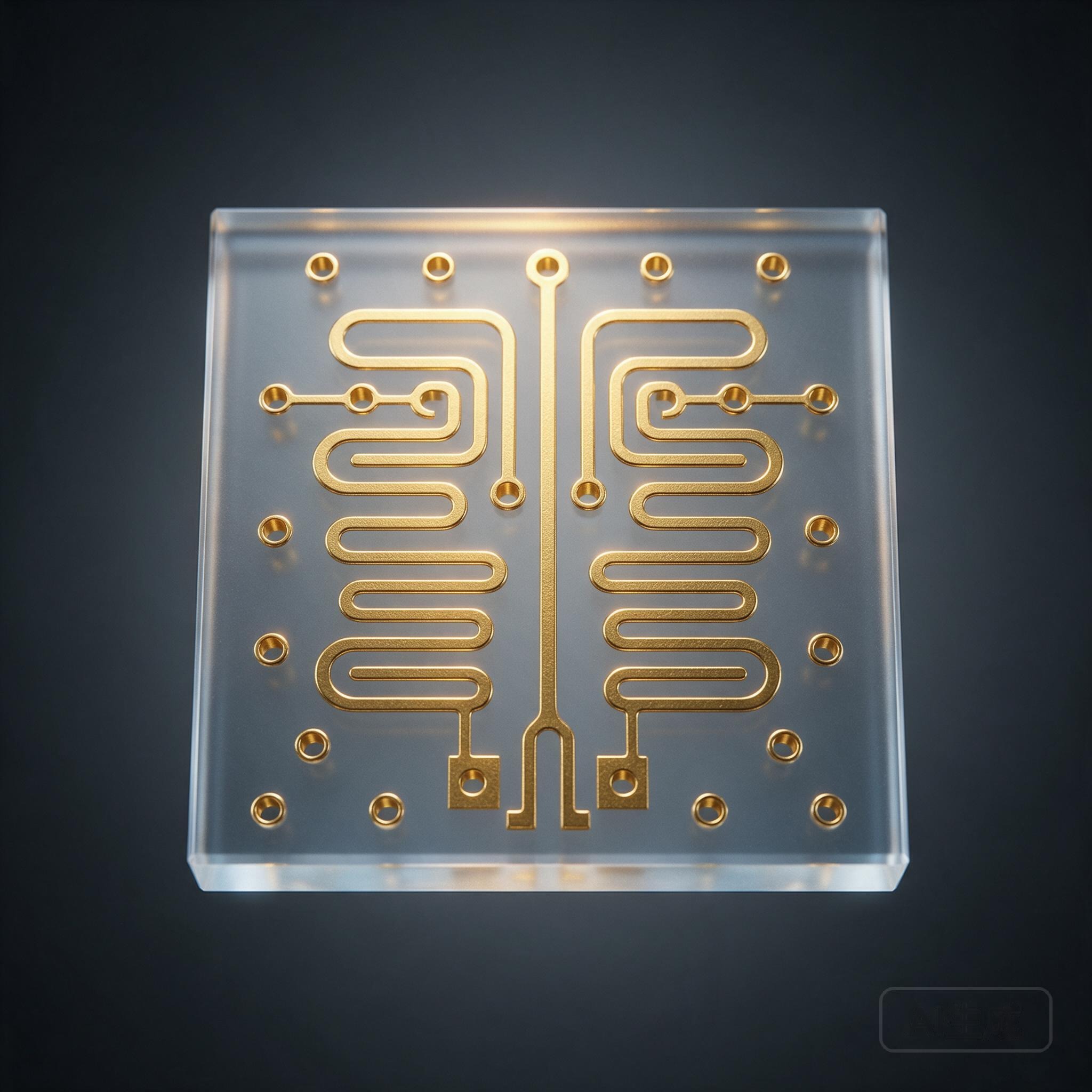
How a thin-film microstrip filter is built
A thin-film filter starts as a polished substrate wafer — typically alumina (εr ≈ 9.9), fused quartz/fused silica (εr ≈ 3.8), or an RF-grade glass (εr ≈ 4–6). The process deposits:
- a backside ground metal, often Au over a Ti/W adhesion layer;
- a top conductor stack (Au, several micrometres thick, plated or evaporated) patterned lithographically into resonators, coupled lines and bond pads;
- optionally thin-film TaN resistors for terminations (for absorptive filters or equalizers);
- MIM capacitors and air bridges where lumped or crossover elements are needed.
The patterned wafer is diced into individual die. Products may ship as bare die for hybrid integration, as wire-bondable parts in open carriers, or as hermetic surface-mount packages. Because conductor dimensions are defined photolithographically, two filters from a wafer have center frequencies that track within a fraction of a percent — a very different regime from manual-tuned cavity filters.
Why the substrate matters
The filter's electrical dimensions scale with 1/√εr, and its insertion loss is set by conductor loss, dielectric loss and radiation.
- Fused silica/quartz combines loss tangent near 0.0001 with low and very stable permittivity. It is the default high-performance choice for stripline/microstrip test fixtures and mmWave, and makes a natural carrier for glass IPDs. Dispersion is low, so filter response is predictable across multi-octave bands.
- Alumina offers higher εr (smaller circuits) and better thermal conductivity, with very low loss when high-purity (99.6%+) material is used. 96% alumina is cheaper but lossier above a few GHz.
- RF glass panels provide a panel-scale economic model borrowed from display manufacturing plus through-glass vias for grounding, enabling wafer/panel-level packaging.
The same supplier will typically characterize every product against measured S-parameters rather than relying solely on EM simulation, which matters because bond-wire and launch parasitics can dominate an otherwise perfect on-die response.
Thin-film vs. LTCC vs. cavity vs. discrete LC
| Filter technology | Typical strengths | Typical limits |
|---|---|---|
| Thin-film microstrip/IPD | Repeatable, small at microwave, low loss, excellent tolerance, customizable geometry | High tooling/NRE for custom designs, bare-die assembly needed |
| LTCC multilayer | High integration, lumped elements, moderate cost at volume | Co-fired shrinkage tolerance, loss above ~30 GHz |
| Cavity/waveguide | Highest Q and power handling | Large, heavy, expensive, manual tuning |
| Discrete LC on PCB | Cheap, easy to tune by handboard | Tolerance, drift, poor at >6 GHz, board-area cost |
| SAW/BAW acoustic | Steep skirts at sub-6 GHz, tiny | Bandwidth and power limits; not wideband microwave |
A common engineering outcome: thin-film microstrip filters take over from LC boards where the band edge precision or insertion loss cannot be met in SMD, and from LTCC where frequency and repeatability dominate; cavities remain for very high-Q, high-power needs such as transmit combiners.
Application patterns
- Switched filter banks and reconfigurable front-ends. Fixed thin-film filters selected by ohmic MEMS or solid-state RF switches provide low-loss multi-band operation. The filter die and switches coexist naturally on a single glass or alumina carrier.
- Instrumentation and test. Spectrum analyzers, signal analyzers and EMC test equipment use thin-film preselector and harmonic filters because unit-to-unit repeatability cuts calibration cost.
- Point-to-point microwave and SATCOM. Compact, hermetically packaged thin-film filters fit directly behind antenna feeds; related products include microstrip and GCPW transmission-line sections used as matching and interconnect elements.
- mmWave 5G and radar front-ends. At n257/n258 and 77 GHz, every 0.1 dB matters and only planar thin-film (or waveguide) structures are practical at the element level.
Integrating a bare-die filter: practical points
- Launch design. Bond-wire inductance detunes the first resonator; use short, multiple downbonds or flip-chip, and model the transition with measured data.
- Cavity and shielding. Microstrip radiates more than stripline; a nearby lid or overmold changes the effective dielectric constant. Maintain the recommended cavity height.
- Ground continuity. Stitch backside ground via through-substrate vias or wrap-arounds; in thin-film microstrip the ground is only as good as its vias.
- Power and power handling. Microstrip edge breakdown and conductor heating set limits; ask for rated CW power at your band and temperature rather than extrapolating from low-frequency tests.
- Reference planes in measurement. Compare datasheet S-parameters on the supplier's specified de-embedding planes; re-simulate with your package launch included.
How to specify
A usable specification contains: passband and edges, maximum passband insertion loss and ripple, rejection at defined offsets (with realistic skirt expectations for the order/topology), impedance and return loss, CW and peak power, temperature range, package (bare die, carrier, SMD hermetic), qualification needs, and mounting process (epoxy/eutectic, bond-wire or flip chip). With those inputs, a thin-film filter can be designed from standard cells on the supplier's process — often faster, and always more repeatable, than tuning a discrete board.
For RF system designers building switched or multi-band front-ends, bare-die thin-film filters on glass or quartz paired with low-loss MEMS switches are one of the highest-leverage combinations available: the same substrate process builds resonators, MIM capacitors, thin-film resistors and spiral inductors, so an entire filter bank can arrive as a single qualified passive die.