Thin-Film RF Resistors, MIM Capacitors and Spiral Inductors: The Building Blocks of an RF IPD
When engineers talk about RF front-ends, the active devices get the attention, but most of the area and a surprising amount of the performance sit in three passive elements: thin-film resistors, metal–insulator–metal (MIM) capacitors, and planar spiral inductors. Fabricated together in thin-film layers on glass, quartz, alumina or high-resistivity silicon, they form the integrated passive device (IPD) that carries matching, biasing, filtering and decoupling around the active die.
This article looks at how each of the three is built, what controls its RF behavior, and why co-integrating them on a low-loss carrier beats a board full of discrete 0201s at microwave and mmWave frequencies.
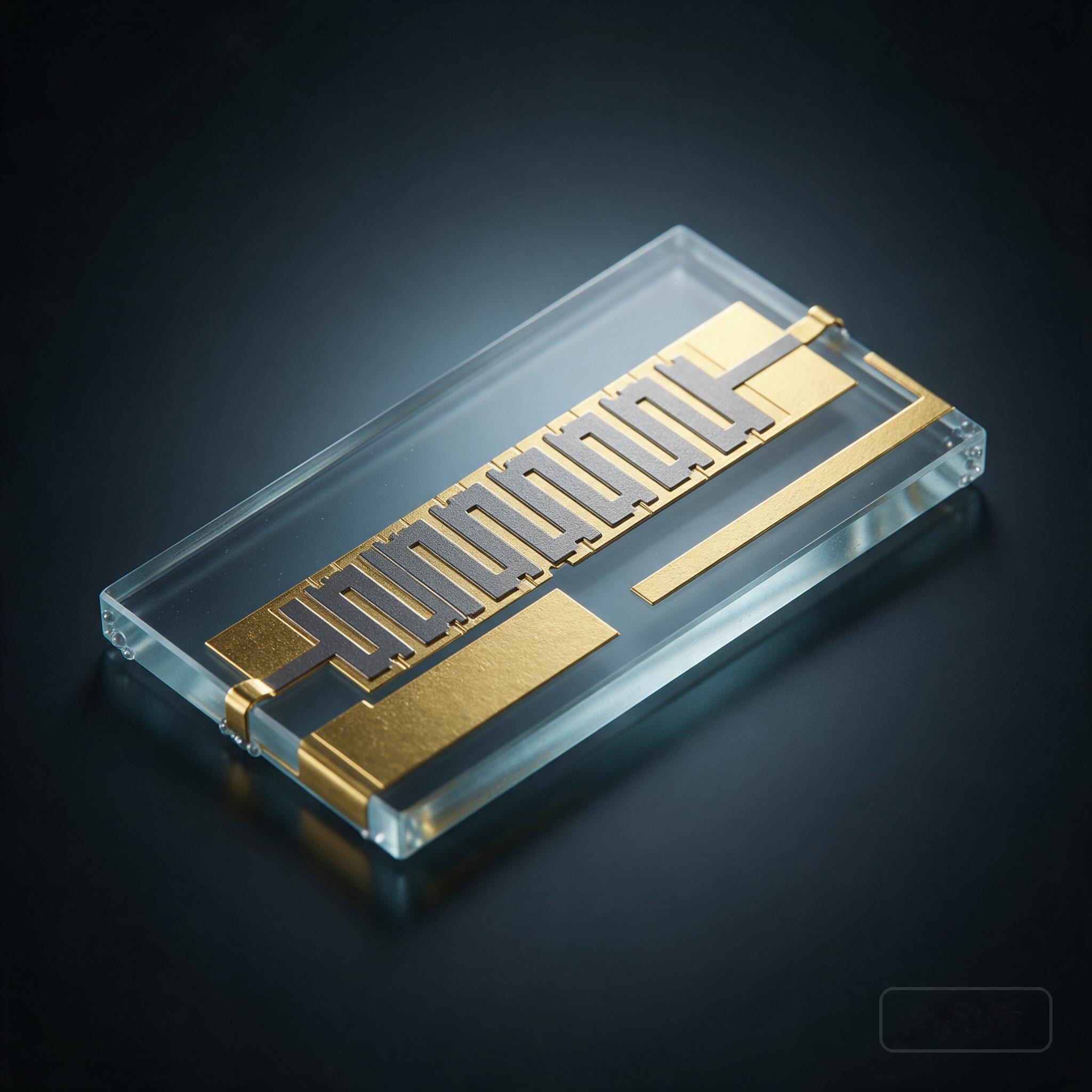
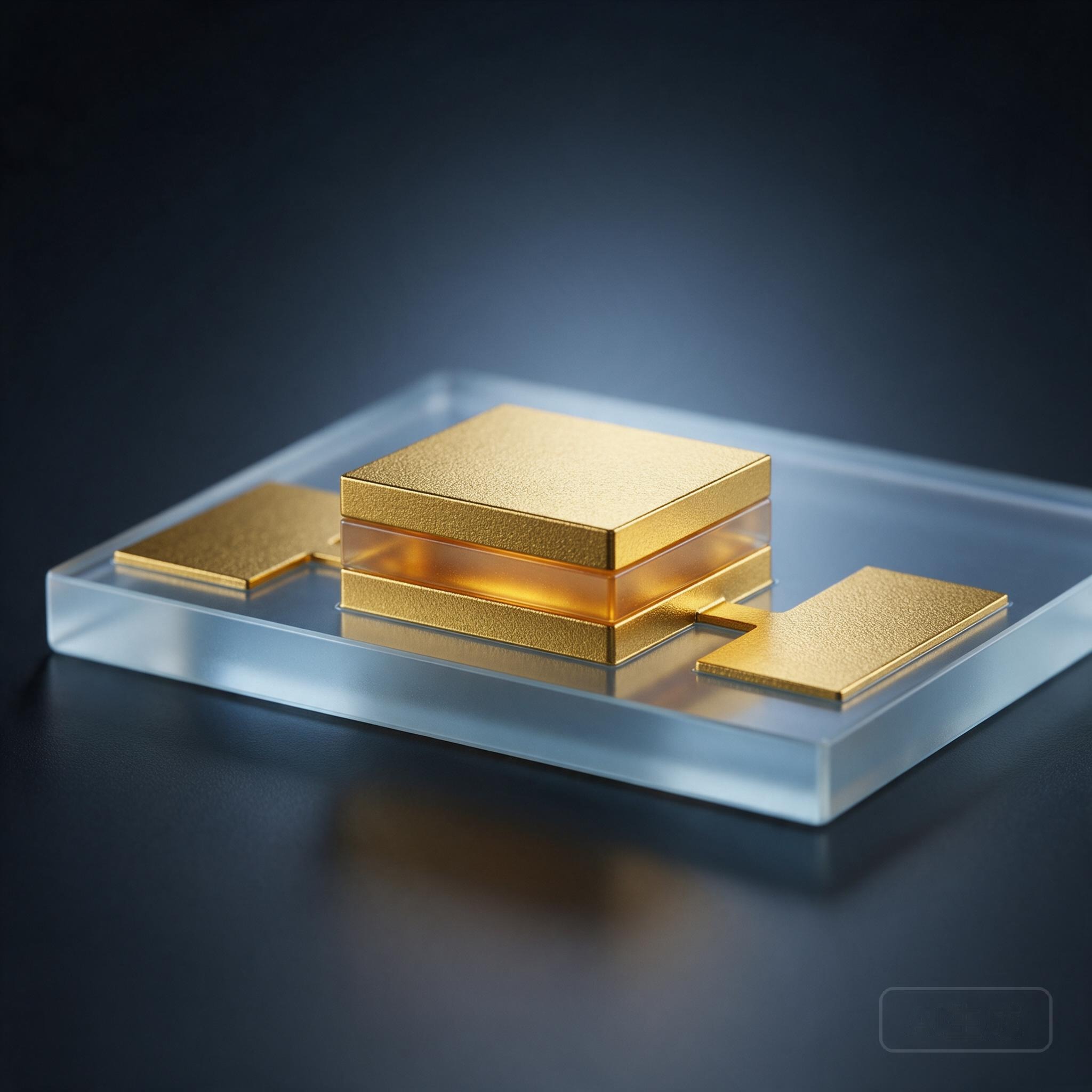
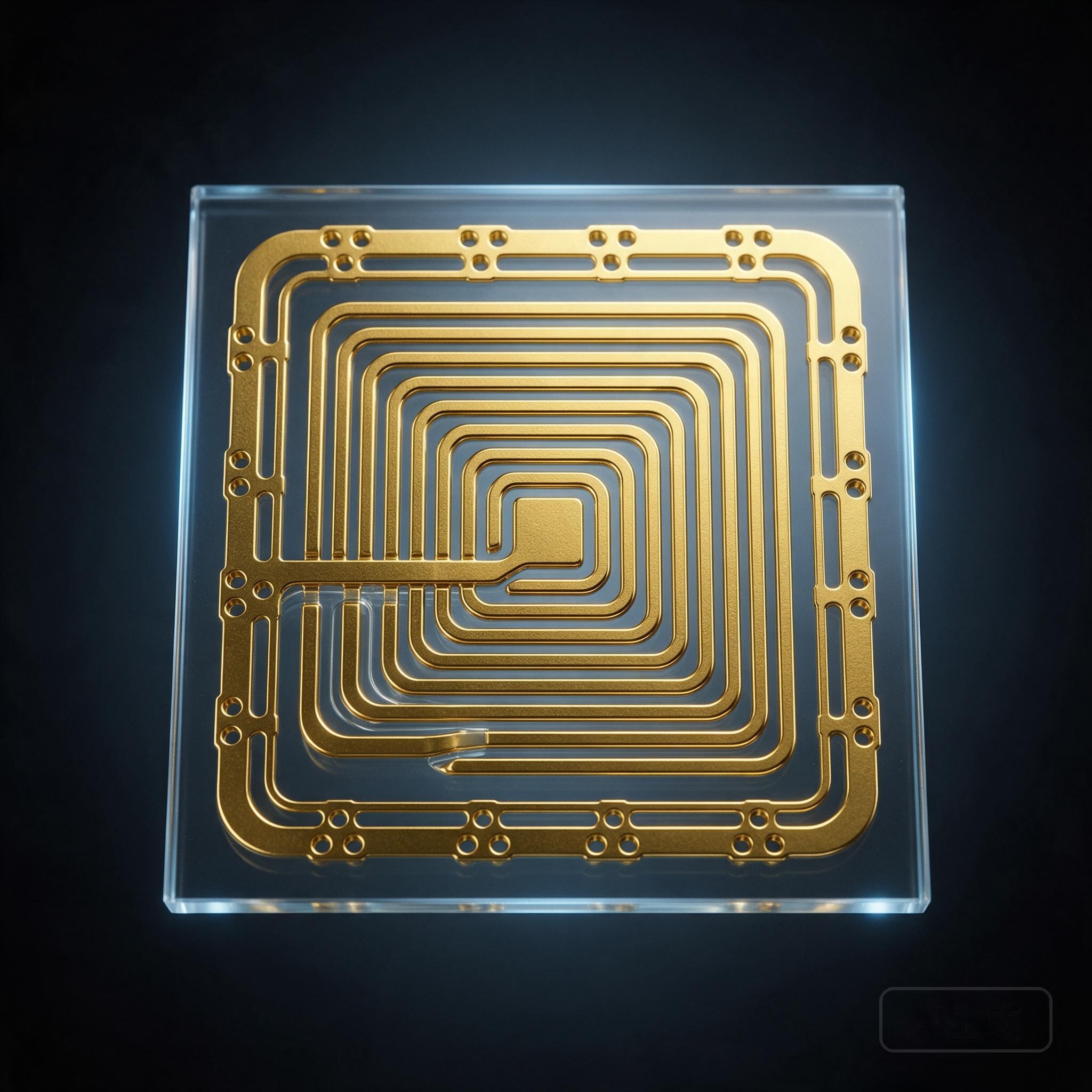
Thin-film resistor: defined by sheet resistance
A thin-film resistor starts as a deposited layer of resistive alloy — tantalum nitride (TaN), nickel-chromium (NiCr), or silicon-chromium (SiCr) — typically tens of nanometres thick. Its designer controls resistance through geometry:
- a long, narrow, serpentine trace raises resistance;
- laser trim or design taps tune the value after processing;
- gold end contacts carry current in and out with minimal parasitic.
What matters at RF is not just the DC value. TaN in particular offers low parasitic capacitance to ground, low temperature coefficient, and low excess noise, which is why it is used for terminations, attenuator pads, feedback and source degeneration in LNAs and PAs, and for the 50 Ω loads in T/R modules. Because the film is patterned lithographically, two resistors on the same wafer match to well under 1% — precision that surface-mount parts cannot reach — which directly improves the balance of differential circuits, hybrids and attenuators.
Power handling is set by film area: at high power, choose wider and/or longer serpentines, multiple parallel resistors, or a higher-thermal-conductivity carrier such as alumina or AlN rather than simply asking for a "higher power" thin-film part.
MIM capacitor: vertical density for matching and bypass
A MIM capacitor stacks two metal plates vertically with a thin, high-quality dielectric (SiN, SiO₂, or a high-k film) between them. This gives much higher capacitance per unit area than an interdigital or planar structure, so MIM capacitors are used wherever real estate matters:
- DC blocking and RF bypass: large value, low series inductance compared with SMD caps;
- matching networks: precise value plus tight tolerance for PA and LNA matches;
- varactor/tuning elements: in MEMS and BST tunable networks, one plate moves or the dielectric permittivity changes;
- bias feed: combined with a high-Z inductor or a quarter-wave stub to form a bias tee.
The figures that govern high-frequency behavior are capacitance density (fF/µm²), dielectric loss tangent, breakdown voltage, and the Q of the plates. At mmWave, the MIM's self-resonance is usually far above the operating frequency precisely because it is so physically small — the opposite problem from a board-mounted ceramic capacitor whose via and mounting inductance dominate.
Spiral inductor: Q is the whole game
The planar spiral — square, octagonal or circular, wound in top metal and brought out through an air-bridge underpass or via to the center — is the only practical way to make nanohenry-to-tens-of-nanohenry inductance on-chip or in thin film. Inductance is set by number of turns, diameter, trace width and spacing; the difficult specification is Q.
Q in a spiral is eaten by:
- metal series resistance, worsened at RF by current crowding and skin effect — thick plated Cu or Au helps;
- substrate losses — eddy currents and displacement current into lossy silicon; this is why glass, fused silica and high-resistivity silicon dramatically outperform standard CMOS silicon for passives;
- eddy currents in the ground plane, mitigated by patterned (slotted) shields or by keeping the inductor over empty substrate;
- mutual coupling to neighbors, enforced through keep-out rules.
High-Q spirals enable the input and output matches of LNAs and PAs, the resonator tanks in tunable filters, the L in lumped-element couplers and baluns, and the choke inductors of bias networks. On a low-loss glass substrate with thick gold, thin-film spirals reach Q values that compete with discrete wirewound parts while remaining batch-fabricated.
Why they are integrated together
Discrete SMD passives are cheap at sub-3 GHz boards, but four trends push designs toward IPD integration:
- Frequency. At Ku band and above, the parasitic inductance of a solder joint is a meaningful fraction of the matching network; integrating shrinks the connection to a lithographic feature.
- Tolerance and matching. Thin-film lithography holds percentage-level tolerances and excellent relative matching, which stabilizes filter center frequencies and balanced circuits.
- Size. A glass-substrate IPD with through-glass vias combines resistor, capacitor, inductor, RDL and ground shielding in one thin part suitable for wafer-level packaging.
- Repeatability and assembly. One placed-and-bonded die replaces dozens of pick-and-place operations, each a potential tombstone or cold-joint failure.
The same technology platform builds all three devices: sputter/evaporate resistive film, plate thick gold, deposit dielectric and a second metal, release air bridges where needed. Adding MEMS switch membranes to the flow then yields fully reconfigurable passive networks on the same carrier.
Specifying integrated passives: a checklist
- Resistors: value, tolerance, power, sheet resistance, temperature coefficient, required trim.
- MIM capacitors: value and tolerance, capacitance density, breakdown, Q at the operating band, self-resonant frequency.
- Inductors: inductance, Q across the band, self-resonance, current rating, keep-out requirements.
- Substrate: glass/fused silica/alumina/HR silicon, thickness, via type, metal stack.
- Package: bare die, wafer-level capped, SMD-form module; bond or flip-chip assembly.
Given the matching network, bias network or filter schematic, a thin-film IPD fabricator can usually map it directly onto a single glass or alumina substrate — and take the discrete BOM count of a microwave front-end down by an order of magnitude while improving RF performance.