Anatomy of a Front-End T/R Module: PA, LNA, Phase Shifter and RF Switch in One Package
Every element of an active electronically scanned array (AESA) — weather radar, satcom-on-the-move, 5G mmWave panels, electronic warfare systems — is driven by a transmit/receive (T/R or TR) module. The T/R module sits between the beamformer/distribution network and the antenna element, and in a single hermetic package it amplifies on transmit, amplifies on receive, sets phase and amplitude, and switches the element between the two paths. Understanding its internal block diagram explains most of the component requirements in a phased array.
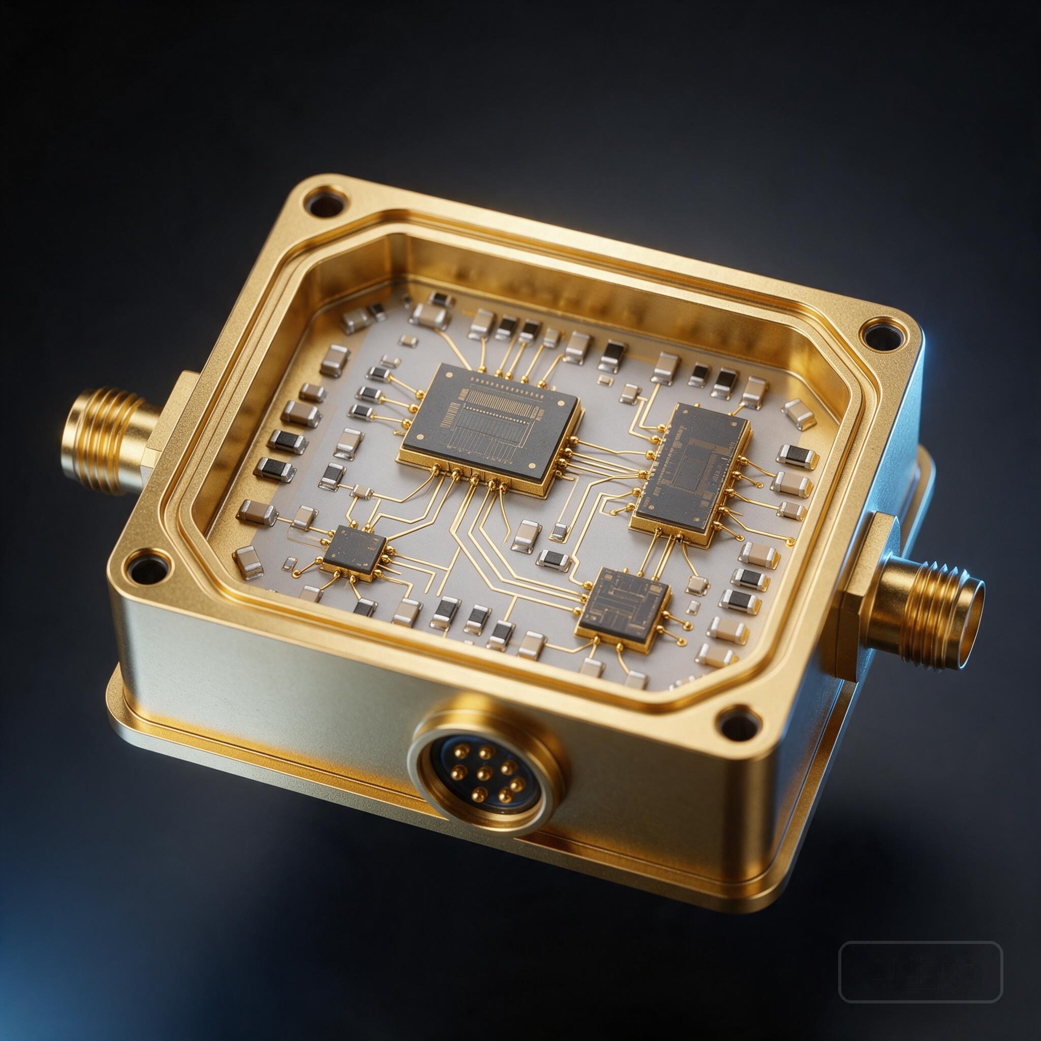
The block diagram
A classic single-channel T/R module contains:
- a power amplifier (PA) for the transmit path;
- a low-noise amplifier (LNA) for the receive path;
- a T/R switch (often a circulator plus switch combination) connecting either PA or LNA to the antenna;
- a phase shifter providing 4–7 bits of phase control for beam steering;
- a variable or switched attenuator (VGA) for amplitude tapering and calibration;
- a transmit driver amplifier and receive limiter;
- bias control, DC-DC conversion, sequencing and telemetry;
- at mmWave, the whole chain may be integrated as a beamformer front-end IC with on-chip T/R switching.
In a receive-only array some blocks disappear; in a large radar the T/R module also contains circulators, limiters and load resistors sized for protection.
Transmit path: PA, matching and the switch
On transmit, the distributed RF feed arrives at the module through a connector or stripline transition, passes through the phase shifter (phase is usually set common to TX and RX), a driver, and then the high-power PA. The PA delivers its output through the T/R switch (or a circulator) to the radiating element.
Key requirements on the transmit side:
- high PAE at the rated output power (every point of PAE multiplied by thousands of elements defines array cooling);
- low insertion loss in the transmit switch — 0.5 dB of switch loss is 0.5 dB off EIRP and watts of heat per element;
- ruggedness into antenna VSWR, including element failures and active VSWR from neighboring radiators.
PA technologies track the frequency: GaN-on-SiC dominates S- to X-band radar for its power density and 50 V operation; GaAs pHEMT covers Ku/Ka and lower-power modules; CMOS/SOI beamformer ICs appear in mass-market Ka-band and 5G n257/n258/n261 panels, often stacked with GaAs PAs for the final stage.
Receive path: the limiter and the LNA set noise figure
On receive, the switch reverses and the signal goes through a limiter (protecting the LNA from the module's own leakage and nearby high-power elements), then the LNA, whose noise figure effectively sets the array's receive sensitivity. After the LNA, a VGA and the common phase shifter condition the signal for the combining network.
Receive chain priorities:
- LNA noise figure, including losses before the LNA (switch, limiter);
- recovery time after transmit bursts (limiter leakage that has not decayed blinds the radar for close targets);
- high-linearity handling of blockers and jammers.
Phase shifters and how the switches are made
Beam steering requires every element's phase to be controllable across 0–360°. Integrated phase shifters are usually one of:
- switched-line / switched filter: RF switches select transmission-line segments or filter states;
- reflection type: 3 dB coupler plus switched reactive loads;
- vector modulator: combines variable-gain quadrature signals (common in silicon beamformers).
The switched-line topology is exactly where high-performance RF switches matter, and MEMS ohmic and capacitive switches have been developed specifically for this role: near-zero DC power, very low insertion loss, and high linearity versus PIN diodes and FETs. A MEMS phase shifter can cut per-element loss and control power compared with a diode version, which in thousands of elements changes the array's thermal and prime-power design. Trade-offs are switching speed (microseconds, adequate for beam steering but not for symbol-level reconfiguration), packaging and hot-switching rules.
Packaging: half the battle
T/R modules are mechanically defined by their package: typically a metal-ceramic or kovar/glass-sealed housing with a brazed multilayer substrate (HTCC/LTCC or thin-film on AlN), die attach, wire bonds or flip chip, hermetic lid seal, and RF connectors (SSMP, SMP, board launch). The package must provide:
- thermal impedance from GaN die to cold plate;
- hermeticity for the MEMS and GaAs die;
- isolation between channels (crosstalk directly raises sidelobes);
- controlled-impedance transitions from coax to stripline to die.
The passive content of the module — thin-film resistors for terminations and loads, MIM capacitors for decoupling and matching, high-Q spiral inductors, and the substrates themselves — increasingly comes from thin-film integrated passive devices on glass or ceramic, which supply tighter tolerance and better Q than discrete 0201/0402 assembly at mmWave.
Array-level design constraints
- Calibration: phase and amplitude states vary over temperature and frequency; modules either store per-element calibration tables or support online calibration.
- Yield and cost: a 5,000-element array multiplies even small per-module yield losses. Standardized modules and relaxed (passively cooled) thermal designs win.
- Reliability: junction temperature of the PA, thermal cycling, and hermetic leak rates dominate field returns.
- Control interface: serial shift registers (SPI-like) or proprietary beamformer buses must load thousands of phase states within the beam-switch time budget.
Quick spec checklist
When evaluating or sourcing a T/R module, collect: frequency band and instantaneous bandwidth; saturated and Psat output power per element; PAE at rated power; receive noise figure including switch/limiter; phase bits and RMS phase/amplitude error; switching time; switching element technology (PIN/FET/MEMS); package size, mass, thermal resistance; control interface; qualification (temperature, vibration, hermeticity). Matching these against the array's EIRP, G/T and scan-angle targets closes the system-to-component loop.