Ohmic vs. Capacitive RF MEMS Switches: How to Choose for 5G, mmWave and Switch Matrices
MEMS contact switches sit at the heart of almost every reconfigurable RF front-end: filter banks, switched-line phase shifters, tunable matching networks, redundant path selection and wideband switch matrices. Once you have decided to use a MEMS switch rather than a PIN diode or an SOI CMOS device, the next design decision is structural — do you need an ohmic-contact switch or a capacitive (capacitive-coupled / shunt) switch? They look similar on a layout (a suspended metal membrane, an electrostatic actuator, a coplanar waveguide), but they conduct, block and fail in very different ways.
This article compares the two contact mechanisms, walks through the electrical consequences for your signal chain, and gives a selection framework for common front-end and instrumentation applications.
The structural difference
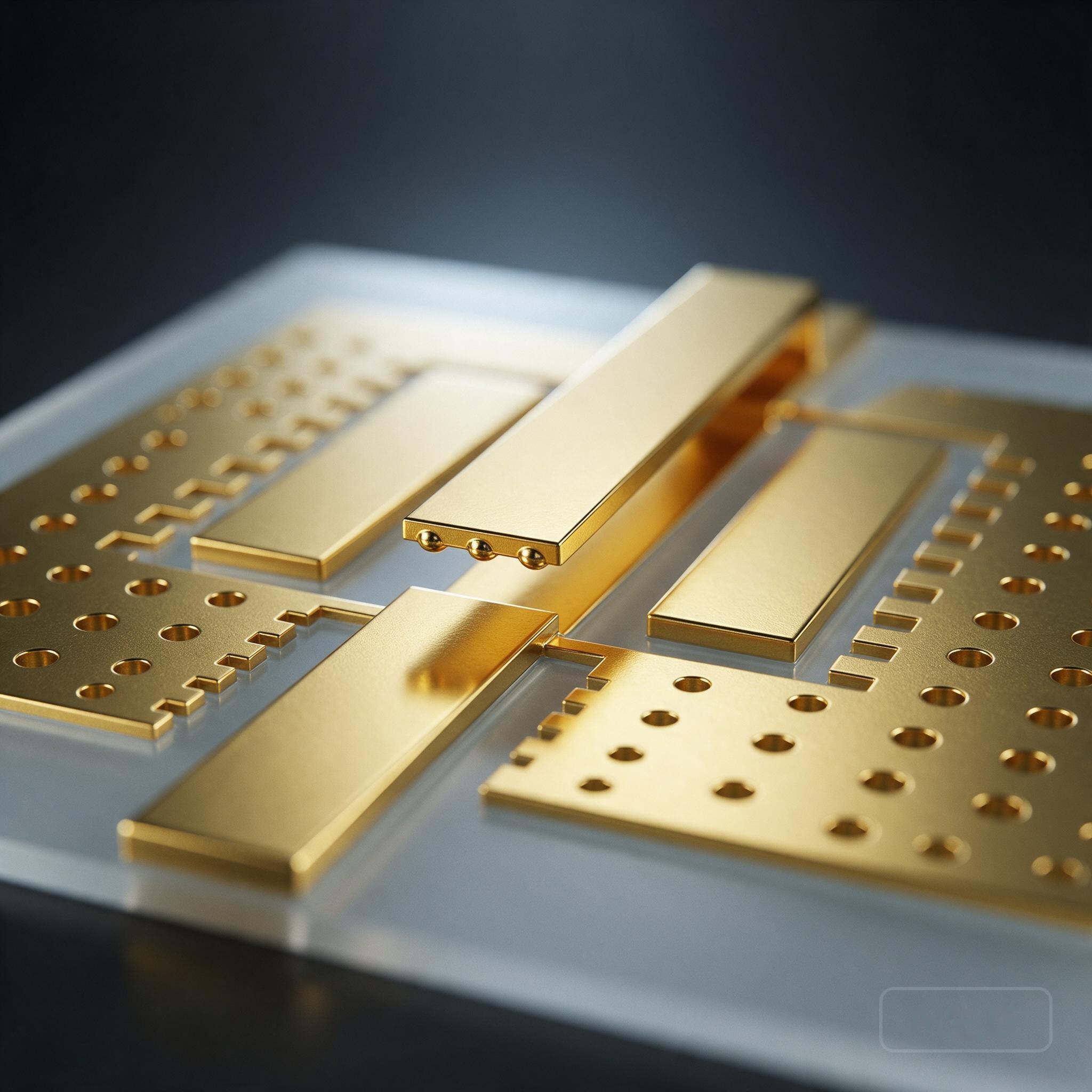
An ohmic-contact series MEMS switch interrupts the signal conductor with a physical gap. A thin metal cantilever or membrane carries one (or several) contact dimples; when an electrostatic voltage pulls the beam down, the dimples touch a metal pad on the signal line and the path closes metallically. With the bias removed, the beam springs back and an air gap isolates the two halves of the line.
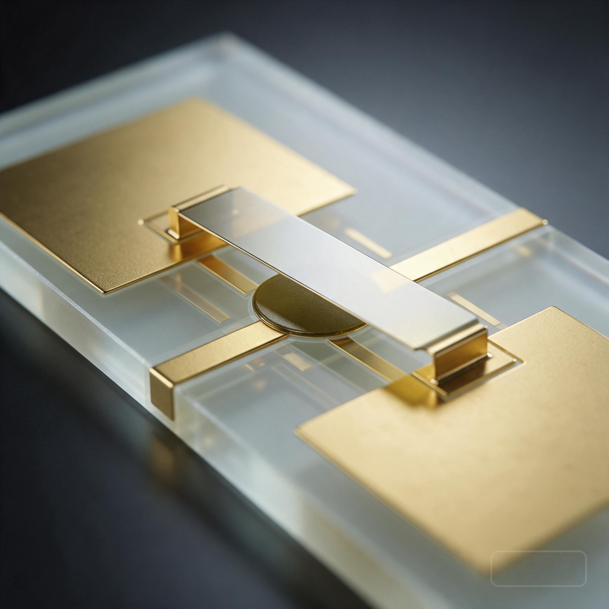
A capacitive shunt MEMS switch never makes DC metal-to-metal contact across the signal path. A membrane bridges a coplanar waveguide; in the up state a thin air gap plus a high-k dielectric patch gives a small capacitance and the RF signal passes underneath. Pulling the membrane down collapses the air gap, the capacitance jumps by a factor of 20–100, and the RF signal is effectively shorted to ground (shunt) or strongly reflected — the switch acts as a near-short at the operating frequency rather than a mechanical open/close.
Insertion loss and isolation: where each topology wins
| Parameter | Ohmic contact | Capacitive shunt |
|---|---|---|
| Conduction mechanism | Direct metal contact | Displacement current through dielectric |
| Frequency sweet spot | DC – 20 GHz and beyond, true wideband | mmWave, roughly 10–100 GHz |
| Up-state loss | Very low (~0.1 dB) when contacts are clean | Very low, limited by membrane parasitics |
| Down-state isolation | High at low frequency, degrades at mmWave | Excellent at the resonant quarter-wave band |
| DC / analog signals | Passes DC | Blocks DC by definition |
The ohmic switch is the only option when the path must carry DC bias, IF signals, baseband, or must work from DC to a high upper frequency with a single part. Its off-state isolation is set by the physical gap and contact geometry, so it behaves well even at 1–6 GHz where a capacitive switch simply cannot develop enough reactance to isolate.
The capacitive switch is frequency selective: the down state reflects best near the LC resonance of the membrane capacitance and the line inductance. At mmWave, where even a few femtofarads matter and wavelengths are short, that resonance can be deliberately placed in-band to deliver 25–40 dB isolation with a simple, contact-free structure.
Power handling and linearity
Both MEMS families need almost no static current and vastly less DC power than PIN diodes, and both are intrinsically more linear than semiconductor junctions — there is no built-in potential and essentially no third-order curvature in the I-V characteristic. That matters for carrier aggregation, full-duplex radio and high-dynamic-range receivers where intermodulation from the switching element directly sets the receiver noise floor.
The details differ:
- Ohmic switches are limited by contact physics. Hot-switching current softens the contact metal, and self-heating at micro-contacts accelerates wear. Conservative designs cold-switch RF, use hard overcoats (Au/Ru, Au/Pt alloys), and derate power.
- Capacitive switches handle no DC current and generally tolerate higher continuous RF power because dissipation is distributed across the dielectric. Their failure modes are dielectric charging (trapped charge shifting the actuation voltage over time) and stiction after long dwell periods, rather than contact erosion.
For hot, high-power transmit switching, ask for the hot-switching power rating explicitly — a "power handling" number on a datasheet may be a cold-switch figure.
Reliability and the contact question
Ohmic-contact reliability is dominated by the contact interface: contamination, contact bounce, material transfer and, in unsealed packages, humidity and organics. Qualified devices are therefore wafer-level capped in dry nitrogen or vacuum, and qualified against mechanical shock and vibration. A well-packaged ohmic MEMS switch will show billions of cold-switch cycles; hot-switch lifetimes are much shorter.
Capacitive switches remove the contact metal pair and therefore the contact erosion failure mode, which makes them attractive for long-life, high-cycle applications such as phase shifters that toggle every beam-steering frame. Their reliability conversation shifts to dielectric quality, charge trapping and membrane fatigue — problems that thin-film process control addresses more predictably over time.
Typical applications
Choose an ohmic-contact MEMS switch for:
- switched filter banks and tunable/reconfigurable filters covering sub-6 GHz through Ku band;
- redundant path and band selection in multi-band front-ends;
- wideband switch matrices and test instrumentation that must pass DC;
- discrete switched-line phase shifters in T/R modules;
- MIM capacitor and resistor bank selection for tunable matching.
Choose a capacitive MEMS switch for:
- mmWave beamforming networks and reflectarray element switching;
- shunt isolation structures in phased-array T/R modules and 5G mmWave panels;
- high-Q varactor tuning where a metal/dielectric/metal capacitor is the desired device;
- very-high-cycle, modest-power applications where contact wear is unacceptable.
Packaging and integration notes
Both devices are fabricated in surface micromachining on high-resistivity silicon, quartz or glass substrates. For designers integrating the bare die, note that the cap cavity and the RF transition dominate final performance, not the membrane alone. Mounting the die on a low-loss carrier such as a fused silica microstrip substrate or a glass IPD preserves the high-Q, low-loss advantage through the package. Hermetic or controlled-atmosphere wafer-level packaging is effectively mandatory for ohmic contacts.
Decision checklist
Before selecting a part, collect: frequency range (DC requirement?), switching configuration (series/shunt), hot- or cold-switching, peak and average RF power, required isolation at the band edge, actuation voltage available, lifetime in cycles, package style, and the linearity target (IP3). Mapping these against the table above resolves most ohmic-versus-capacitive questions on the first pass.
If your architecture mixes sub-6 GHz filter switching with mmWave beam steering, the answer is often both: ohmic devices in the low-band front-end and capacitive structures in the mmWave aperture. For fixed-frequency, wideband and DC-carrying paths, start with ohmic; for resonant mmWave and ultra-high-cycle shunt applications, start capacitive.